This is the official manual transcribed from PDF. Enjoy!
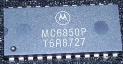
MOTOROLA MC6850 ASYNCHRONOUS COMMUNICATIONS INTERFACE ADAPTER (ACIA)
v0.8
The MC6850 Asynchronous Communications Interface Adapter provides the data formatting and control to interface serial asynchronous data communications information to bus organized systems such as the MC6800 Microprocessing Unit.
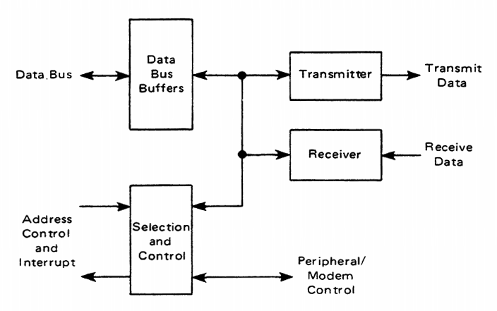
The bus interface of the MC6850 includes select, enable, read/write, interrupt and bus interface logic to allow data transfer over an 8-bit bidirectional data bus. The parallel data of the bus system is serially transmitted and received by the asynchronous data interface, with proper formatting and error checking The functional configuration of the ACIA is programmed via the data bus during system initialization. A programmable Control Register provides variable word lengths, clock division ratios, transmit control, receive control, and interrupt control. For peripheral or modem operation, three control lines are provided. These lines allow the ACIA to interface directly with the MC6860L 0-600 bps digital modem.
- 8- and 9- Bit Transmission
- Optional Even and Odd Parity
- Parity, Overrun and Framing Error Checking
- Programmable Control Register
- Optional ÷1, ÷16, and ÷64 Clock Modes
- Up to 1.0 Mbps Transmission
- False Start Bit Deletion
- Peripheral/ Modem Control Functions
- Double Buffered
- One- or Two-Stop Bit Operation
MC6850 ASYNCHRONOUS COMMUNICATIONS INTERFACE ADAPTER BLOCK DIAGRAM

Pin assignment
| Func | Pin | Pin | Func | |
|---|---|---|---|---|
| VSS | 1 | ##U## | 24 | CTS |
| Rx Data | 2 | ##### | 23 | DCD |
| Rx CLK | 3 | ##### | 22 | D0 |
| Tx CLK | 4 | ##### | 21 | D1 |
| RTS | 5 | ##### | 20 | D2 |
| Tx Data | 6 | ##### | 19 | D3 |
| IRQ | 7 | ##### | 18 | D4 |
| CS0 | 8 | ##### | 17 | D5 |
| CS2 | 9 | ##### | 16 | D6 |
| CS1 | 10 | ##### | 15 | D7 |
| RS | 11 | ##### | 14 | E |
| VCC | 12 | ##### | 13 | R/W |
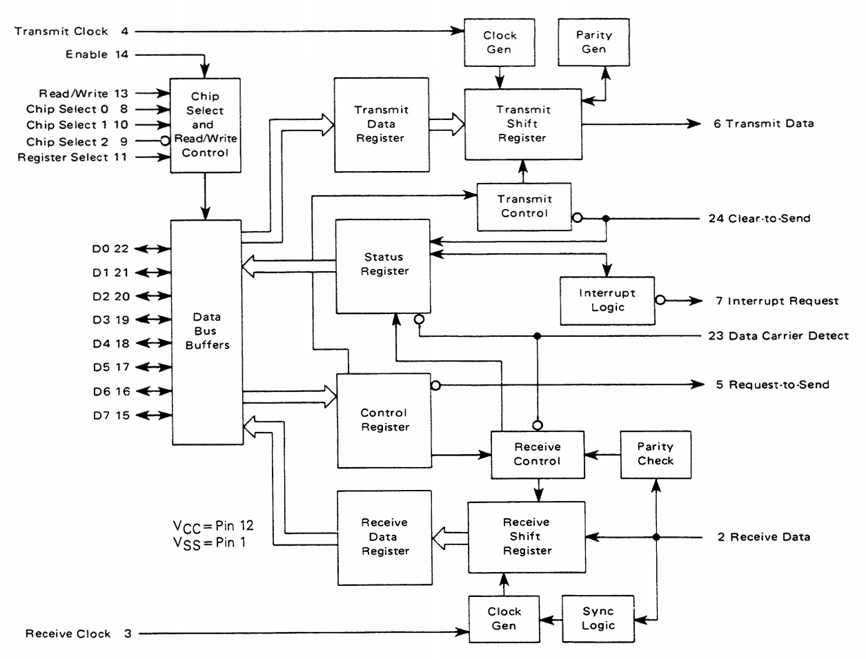
EXPANDED BLOCK DIAGRAM

DEVICE OPERATION
At the bus interface, the ACIA appears as two addressable memory locations. Internally, there are four registers: two read only and two write-only registers. The read-only registers are Status and Receive Data; the write-only registers are Control and Transmit Data. The serial interface consists of serial input and output lines with independent docks, and three peripheral/modem control lines.
MASTER RESET
The master reset (CRO, CR1) should be set during system initialization to insure the reset condition and prepare for programming the ACIA functional configuration when the communications channel is required. During the first master reset, the (IRQ and (RTS outputs are held at level 1. On all other master resets, the (RTS output can be programmed high or low with the (IRQ output held high. Control bits CR5 and CR6 should also be programmed to define the state of RTS whenever master reset is utilized. The ACIA also contains internal power-on reset logic to detect the power line turn-on transition and hold the chip in a reset state to prevent erroneous output transitions prior to initialization. This circuitry depends on clean power turn-on transitions. The power-on reset is released by means of the bus-programmed master reset which must be applied prior to operating the ACIA. After master resetting the ACIA. The programmable Control Register can be set for a number of options such as variable clock divider ratios, variable word length, one or two stop bits, parity (even, odd, or none).
TRANSMIT
A typical transmitting sequence consists of reading the ACIA Status Register either as a result of an interrupt or in the ACIA’s turn in a polling sequence. A character may be written into the Transmit Data Register if the status read operation has indicated that the Transmit Data Register is empty. This character is transferred to a Shift Register where it is serialized and transmitted from the Transmit Data output preceded by a start bit and followed by one or two stop bits. Internal parity (odd or even) can be optionally added to the character and will occur between the last data bit and the first stop bit. After the first character is written in the Data Register, the Status Register can be read again to check for a Transmit Data Register Empty condition and current peripheral status. If the register is empty, another character can be loaded for transmission even though the first character is in the process of being transmitted (because of double buffering). The second character will be automatically transferred into the Shift Register when the first character transmission is completed. This sequence continues until all the characters have been transmitted.
RECEIVE
Data is received from a peripheral by means of the Receive Data input. A divide-by-one clock ratio is provided for an externally synchronized clock (to its data) while the divide by-16 and 64 ratios are provided for internal synchronization. Bit synchronization in the divide-by-16 and 64 modes is initiated by the detection of 8 or 32 low samples on the receive line in the divide by 16 and 64 modes respectively. False start bit deletion capability insures that a full half bit of a start bit has been received before the internal clock is synchronized to the bit time. As a character is being received, parity (odd or even) will be checked and the error indication will be available in the Status Register along with framing error, overrun error, and Receive Data Register full. In a typical receiving sequence, the Status Register is read to determine if a character has been received from a peripheral. If the Receiver Data Register is full, the character is placed on the 8-bit ACIA bus when a Read Data command is received from the MPU. When parity has been selected for a 7-bit word (7 bits plus parity), the receiver strips the parity bit (D7=0) so that data alone is transferred to the MPU. This feature reduces MPU programming. The Status Register can continue to be read to determine when another character is available in the Receive Data Register. The receiver is also double buffered so that a character can be read from the data register as another character is being received in the shift register. The above sequence continues until all characters have been received.
INPUT/OUTPUT FUNCTIONS
ACIA INTERFACE SIGNALS FOR MPU
The ACIA interfaces to the M6800 MPU with an 8-bit bidirectional data bus, three chip select lines, a register select line, an interrupt request line, read/write line, and enable line. These signals permit the MPU to have complete control over the ACIA.
ACIA Bidirectional Data (D0-D7)
The bidirectional data lines (D0-D7) allow for data transfer between the ACIA and the MPU. The data bus output drivers are three-state devices that remain in the high-impedance (off) state except when the MPU performs an ACIA read operation.
ACIA Enable (E)
The Enable signal, E, is a high-impedance TTL compatible input that enables the bus input/output data buffers and clocks data to and from the ACIA. This signal will normally be a derivative of the MC6800 φ2 Clock or MC6809 E clock.
Read/Write (R/W)
The Read/Write line is a high-impedance input that is TTL compatible and is used to control the direction of data flow through the ACIA’s input/ output data bus interface. When Read/Write is high (MPU Read cycle), ACIA output drivers are turned on and a selected register is read When it is low, the ACIA output drivers are turned off and the MPU writes into a selected register Therefore, the Read/Wnte signal is used to select read-only or write-only registers within the ACIA.
Chip Select (CS0, CS1, CS2)
These three high impedance TTL-compatible input lines are used to address the ACIA . The ACIA is selected when CS0:and CS1 are high and CS2 is low. Transfers of data to and from the ACIA are then performed under the control of the Enable Signal, Read Write, and Register Select.
Register Select (RS)
The Register Select line is a high-impedance input that is TTL compatible. A high level is used to select the Transmit/Receive Data Registers and a low level the Control/Status Registers. The Read/Write signal line is used in conjunction with Register Select to select the read-only or write-only register in each register pair.
Interrupt Request (IRQ)
Interrupt Request is a TTL-compatible, open-drain (no internal pullup), active low output that is used to interrupt the MPU. The IRQ output remains low as long as the cause of the interrupt is present and the appropriate interrupt enable within the ACIA is set The IRQ status bit, when high, indicates the IRQ output is in the active state.
Interrupts result from conditions in both the transmitter and receiver sections of the ACIA. The transmitter section causes an interrupt when the Transmitter Interrupt Enabled condition is selected (CR5•CR6), and the Transmit Data Register Empty (TDRE) status bit is high. The TDRE status bit indicates the current status of the Transmitter Data Register except when inhibited by Clear-to-Send (CTS) being high or the ACIA being maintained in the Reset condition. The interrupt is cleared by writing data into the Transmit Data Register. The interrupt is masked by disabling the Transmitter Interrupt via CR5 or CR6 or by the loss of CTS which inhibits the TDRE status bit. The Receiver section causes an interrupt when the Receiver Interrupt Enable is set and the Receive Data Register Full (RDRF) status bit is high, an Overrun has occurred, or Data Carrier Detect (DCD) has gone high. An interrupt resulting from the RDRF status bit can be cleared by reading data or re setting the ACIA. Interrupts caused by Overrun or loss of DCD are cleared by reading the status register after the error condition has occurred and then reading the Receive Data Register or resetting the ACIA. The receiver interrupt is masked by resetting the Receiver Interrupt Enable.
CLOCK INPUTS
Separate high-impedance TTL-compatible inputs are provided for clocking of transmitted and received data. Clock frequencies of 1, 16, or 64 times the data rate may be selected.
Transmit Clock (Tx CLK)
The Transmit Clock input is used for the clocking of transmitted data. The transmitter initiates data on the negative transition of the clock.
Receive Clock (Rx CLK)
The Receive Clock input is used for synchronization of received data. (In the ÷1 mode, the clock and data must be synchronized externally.) The receiver samples the data on the positive transition of the clock.
SERIAL INPUT/OUTPUT LINES
Receive Data (Rx Data)
The Receive Data line is a high-impedance TTL-compatible input through which data is received in a serial format. Synchronization with a clock for detection of data is accomplished internally when clock rates of 16 or 64 times the bit rate are used.
Transmit Data (Tx Data)
The Transmit Data output line transfers serial data to a modem or other peripheral.
PERIPHERAL/MODEM CONTROL
The ACIA includes several functions that permit limited control of a peripheral or modem. The functions included are Clear-to-Send, Request-to-Send and Data Carrier Detect.
Clear-to-Send (CTS)
This high impedance TTL-compatible input provides automatic control of the transmitting end of a communications link via the modem Clear-to-Send active low output by inhibiting the Transmit Data Register Empty (TDRE) status bit.
Request-to-Send (RTS)
The Request-to-Send output enables the MPU to control a peripheral or modem via the data bus. The RTS output corresponds to the state of the Control Register bits CR5 and CR6. When CR6=0 or both CR5 and CR6=1, the RTS output is low (the active state). This output can also be used for Data Terminal Ready (DTR).
Data Carrier Detect (DCD)
This high-impedance TTL-compatible input provides automatic control, such as in the receiving end of a communications link by means of a modem Data Carrier Detect output. The DCD input inhibits and initializes the receiver section of the ACIA when high A low-to-high transition of the Data Carrier Detect initiates an interrupt to the MPU to indicate the occurrence of a loss of carrier when the Receive Interrupt Enable bit is set. The Rx CLK must be running for proper DCD operation.
ACIA REGISTERS
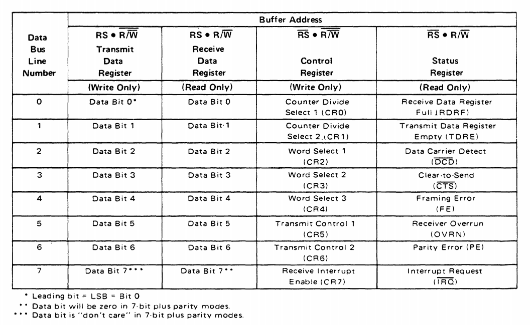
The expanded block diagram for the ACIA indicates the internal registers on the chip that are used for the status, control. receiving, and transmitting of data. The content of each of the registers is summarized in Table 1.
TRANSMIT DATA REGISTER (TDR)
Data is written in the Transmit Data Register during the negative transition of the enable (E) when the ACIA has been addressed with RS high and R/W low. Writing data into the register causes the Transmit Data Register Empty bit in the Status Register to go low. Data can then be transmitted. If the transmitter is idling and no character is being transmitted, then the transfer will take place within 1-bit time of the trailing edge of the Write command. If a character is being transmitted, the new data character will commence as soon as the previous character is complete. The transfer of data causes the Transmit Data Register Empty (TDRE) bit to indicate empty.
RECEIVE DATA REGISTER (RDR)
Data is automatically transferred to the empty Receive Data Register (RDR) from the receiver deserializer (a shift register) upon receiving a complete character. This event causes the Receive Data Register Full bit (RDRF) in the status buffer to go high (full). Data may then be read through the bus by addressing the ACIA and selecting the Receive Data Register with RS and R/W high when the ACIA is enabled. The non destructive read cycle causes the RDRF bit to be cleared to empty although the data is retained in the RDR. The status is maintained by RDRF as to whether or not the data is current. When the Receive Data Register is full, the automatic transfer of data from the Receiver Shift Register to the Data Register is inhibited and the RDR contents remain valid with its current status stored in the Status Register.
TABLE 1 - DEFINITION OF ACIA REGISTER CONTENTS

CONTROL REGISTER
The ACIA Control Register consists of eighty bits of write-only buffer that are selected when RS and R/W are low. This register controls the function of the receiver, transmitter, interrupt enables, and the Request-to-Send peripheral/modem control output.
Counter Divide Select Bits (CRO and CR1)
The Counter Divide Select Bits (CRO and CR1) determine the divide ratios utilized in both the transmitter and receiver sections of the ACIA. Additionally, these bits are used to provide a master reset for the ACIA which clears the Status Register (except for external conditions on CTS and DCD) and initializes both the receiver and transmitter. Master reset does not affect other Control Register bits. Note that after power-on or a power fail/restart, these bits must be set high to reset the ACIA. After resetting, the clock divide ratio may be selected. These counter select bits provide for the following clock divide ratios:
| CR1 | CR0 | Function |
|---|---|---|
| 0 | 0 | ÷1 |
| 0 | 1 | ÷16 |
| 1 | 0 | ÷64 |
| 1 | 1 | Master Reset |
Word Select Bits (CR2, CR3, end CR4)
The Word Select bits are used to select word length, parity, and the number of stop bits. The encoding format is as follows:
| CR4 | CR3 | CR2 | Function |
|---|---|---|---|
| 0 | 0 | 0 | 7 Bits + Even Parity + 2 Stop Bits |
| 0 | 0 | 1 | 7 Bits + Odd Parity + 2 Stop Bits |
| 0 | 1 | 0 | 7 Bits + Even Parity + 1 Stop Bit |
| 0 | 1 | 1 | 7 Bits + Odd Parity + 1 Stop Bit |
| 1 | 0 | 0 | 8 Bits + 2 Stop Bits |
| 1 | 0 | 1 | 8 bits + 1 Stop Bit |
| 1 | 1 | 0 | 8 Bits + Even parity + 1 Stop Bit |
| 1 | 1 | 1 | 8 Bits + Odd Parity + 1 Stop Bit |
Word length, Parity Select, and Stop Bit changes are not buffered and therefore become effective immediately.
Transmitter Control Bits (CR5 and CR6)
Two Transmitter Control bits provide for the control of the interrupt from the Transmit Data Register Empty condition, the Request-to-Send (RTS) output, and the transmission of a Break level (space). The following encoding format is used:
| CR6 | CR5 | Function |
|---|---|---|
| 0 | 0 | RTS=low, Transmitting Interrupt Disabled. |
| 0 | 1 | RTS=low, Transmitting Interrupt Enabled. |
| 1 | 0 | RTS=high, Transmitting Interrupt Disabled. |
| 1 | 1 | RTS=low, Transmits a Break level on the Transmit Data Output. Transmitting Interrupt Disabled. |
Receive Interrupt Enable Bit (CR7)
The following interrupts will be enabled by a high level in bit position 7 of the Control Register (CR7): Receive Data Register Full, Overrun, or a low-to-high transition on the Data Carrier Detect (DCD) signal line.
STATUS REGISTER
Information on the status of the ACIA is available to the MPU by reading the ACIA Status Register. This read-only register is selected when RS is low and R/W is high. Information stored in this register indicates the status of the Transmit Data Register, the Receive Data Register and error logic, and the peripheral/modem status inputs of the ACIA.
Receive Data Register Full (RDRF), Bit 0
Receive Data Register Full indicates that received data has been transferred to the Receive Data Register. RDRF is cleared after an MPU read of the Receive Data Register or by a master reset. The cleared or empty state indicates that the contents of the Receive Data Register are not current, Data Carrier Detect being high also causes RDRF to indicate empty.
Transmit Data Register Empty (TDRE), Bit 1
The Transmit Data Register Empty bit being set high indicates that the Transmit Data Register contents have been transferred and that new data may be entered. The low state indicates that the register is full and that transmission of a new character has not begun since the last write data command.
Data Carrier Detect (DCD), Bit 2
The Data Carrier Detect bit will be high when the DCD input from a modem has gone high to indicate that a carrier is not present. This bit going high causes an Interrupt Request to be generated when the Receive Interrupt Enable is set. It remains high after the DCD input is returned low until cleared by first reading the Status Register and then the Data Register or until a master reset occurs. If the DCD input remains high after read status and read data or master reset has occurred, the interrupt is cleared, the DCD status bit remains high and will follow the input.
Clear-to-Send (CTS), Bit 3
The Clear-to-Send bit indicates the state of the Clear-to-Send input from a modem. A low CTS indicates that there is a Clear-to-Send from the modem. In the high state, the Transmit Data Register Empty bit is inhibited and the Clear-to-Send status bit will be high Master reset does not affect the Clear-to-Send status bit.
Framing Error (FE), Bit 4
Framing error indicates that the received character is improperly framed by a start and a stop bit and is detected by the absence of the first stop bit. This error indicates a synchronization error, faulty transmission, or a break condition. The framing error flag is set or reset during the receive data transfer time. Therefore, this error indicator is present throughout the time that the associated character is available.
Receiver Overrun (OVRN), Bit 5
Overrun is an error flag that indicates that one or more characters in the data stream were lost. That is, a character or a number of characters were received but not read from the Receive Data Register (RDR) prior to subsequent characters being received. The overrun condition begins at the midpoint of the last bit of the second character received in succession without a read of the RDR having occurred. The Overrun does not occur in the Status Register until the valid character prior to Overrun has been read. The RDRF bil remains set untit the Overrun is reset Character synchronization is maintained during the Overrun condition. The Overrun indication is reset after the reading of data from the Receive Data Register or by a Master Reset.
Parity Error (PE), Bit 6
The parity error flag indicates that the number of highs (ones) in the character does not agree with the preselected odd or even parity. Odd parity is defined to be when the total number of ones is odd. The parity error indication will be present as long as the data character is in the RDR. If no parity is selected, then both the transmitter parity generator output and the receiver parity check results are inhibited.
Interrupt Request (IRQ), Bit 7
The IRQ bit indicates the state of the IRQ output. Any interrupt condition with its applicable enable will be indicated in this status bit. Anytime the IRQ output is low the IRQ bit will be high to indicate the interrupt or service request status. IRQ is cleared by a read operation to the Receive Data Register or a write operation to the Transmit Data Register.
AFTERWORD
This datasheet has been converted using an OCR’ed version hosted on The Internet Archive with the original document here. If you spot any errors due to the transcribing, we welcome any corrections!